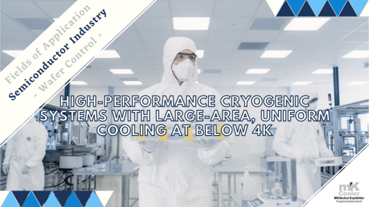
Wafer control
©Niklas Guenther via Canva.com
For the semiconductor industry, it is envisaged to design cryogenic systems with high performance and with large-area, uniform cooling at below 4K, i.e. e.g. down to around 1K or less.
Such systems would be very helpful for classical wafer production (silicon), and even necessary for the coming wafer production (quantum computing etc.), as the following considerations show:
In the race to produce the most powerful quantum computers, two trends have been discernible for several years.
One group of companies in this race, which includes IBM, Microsoft and Google, is relying on "superconducting materials" to realise the qubits. The other group, which includes Intel in particular, relies on qubits made of "ultra-pure silicon material".
In both cases, new and higher demands will be placed on "wafer inspection systems". Either because the qubits can only be operated and thus examined in a superconducting state anyway, or because the high-purity silicon structures can only really be examined for defects in all precision at very low temperatures.
In addition, it is clear to all development groups that quantum computers will only be of broad use if they have millions rather than just thousands of qubits. This predicts that "planar inspection systems" will again be needed in the future.